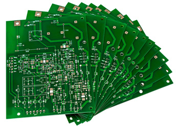
A double-sided PCB, also known as a double-layer or two-layer PCB, features copper layers on both sides of the board.
Compared to single-sided PCBs, double-sided PCBs offer increased sophistication and adaptability, allowing for more complex circuits and higher component density.
The construction of a double-sided PCB starts with a non-conductive base, typically made of fiberglass-reinforced epoxy known as FR-4, providing insulation and mechanical support
Thin copper layers are laminated onto both sides of the substrate to form the conductive layers of the PCB.
The desired circuitry pattern, including traces, pads, and other copper features, is etched into these copper layers to create the final PCB design.
The copper layers on both sides of the PCB are electrically insulated from each other to prevent short circuits and ensure proper routing.
Insulation is achieved by applying a layer of non-conductive material known as solder mask or solder resist. This protective layer covers the copper traces and pads, leaving only the required areas exposed for soldering components
Advantages of Double-Sided PCBs
Enhanced Complexity and Density:
Double-sided PCBs excel in enabling higher levels of circuit complexity and increased component density compared to single-sided PCBs.
Expanded Routing Options:
Designers benefit from the presence of copper layers on both sides of the board, which provides them with a wider array of routing choices. This flexibility allows for the accommodation of more components and intricate interconnections.
Versatile Applications:
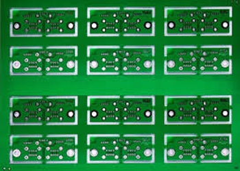
Double-sided PCBs find application across diverse industries, including industrial machinery and consumer electronics. Their enhanced capabilities make them suitable for a wide range of scenarios and requirements.
Get in touch with us
Like to have a cup of coffee with us, to discuss something interesting and innovative,
Please complete the below form and we are here with you.