● Fundamental type of PCB used for simple electronic circuits and cost-effective applications.
Construction Process:
● Begins with a non-conductive substrate.
● Substrate provides mechanical support and insulation.
● Conductive layer formed by laminating thin copper onto substrate.
● Copper traces often covered by solder mask (protective substance), except for soldering areas.
Advantages
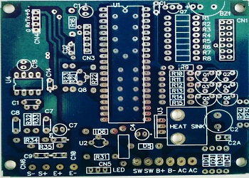
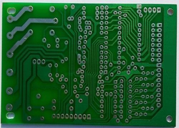
● A single-sided PCB, also known as a single-layer or one-layer PCB, contains only one copper layer on one side.
● It is the simplest and most fundamental type of PCB, commonly used for straightforward electronic circuits and cost-effective applications.
● The construction of a single-sided PCB starts with a non-conductive substrate, typically made of fiberglass-reinforced epoxy known as FR-4, providing mechanical support and insulation.
● The conductive layer is formed by laminating a thin copper sheet onto the substrate.
● Copper traces on this layer are usually covered by a protective substance called solder mask, leaving areas exposed for soldering.
Advantages, Preferences, and Constraints of
Single-Sided PCBs
Simplicity and Affordability: Single-sided PCBs offer key advantages in terms of simplicity and affordability. The production process is streamlined compared to multilayer PCBs, as it involves only one copper layer. This leads to fewer processes and less need for sophisticated machinery.
Preferred for Basic Electronics: Single-sided PCBs are a popular choice for applications involving basic electronic devices, consumer electronics, and low-volume production. Their straightforward design contributes to reduced production costs.
Design Limitations: The single-layer design does impose limitations on circuit complexity and density. With just one copper layer, there's limited space for routing traces and placing components. Consequently, intricate circuits with multiple components and complex connections are less suitable for single-sided PCBs.
Space Constraints: Due to the single-layer configuration, there can be challenges in accommodating intricate layouts. This might result in larger board dimensions and less efficient utilization of available space.
Get in touch with us
Like to have a cup of coffee with us, to discuss something interesting and innovative,
Please complete the below form and we are here with you.